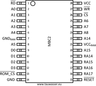
MBC2
Nintendo's MBC2 can be used to address up to 2 Mbit of ROM and 512×4 bit of internal RAM.
Pinout
| Pin No. | Name | Type | Comment |
|---|---|---|---|
| 28 | VCC | PWR | I/O + logic 5V supply |
| 14 | GND | PWR | I/O + logic Ground supply |
| 21 | VCC_RAM | PWR | RAM supply |
| 7 | GND_RAM | PWR | RAM Ground supply |
| 12–9 | D3–D0 | I/O | Data Bus |
| 1 | RD | I | Low-Active Read Enable |
| 27 | WR | I | Low-Active Write Enable |
| 26 | CS | I | Low-Active Chip Select |
| 15 | RESET | I | Low-Active Asynchronous Reset |
| 20, 22–25, 8, 6–2 | A15–A14, A8–A0 | I | Address Bus |
| 16–19 | RA17–RA14 | O | Upper ROM Address Lines |
| 13 | ROM_CS | O | Low-Active ROM Chip Select |
Footprint: SOP127P1200X225-24
Remarks: All I/O pins are protected via diodes to VCC/GND. VCC and VCC_RAM both supply RAM -- probably depending on VCC voltage.
Registers
Write-Accessible Registers:
- 0b00-- ---0 ---- ----: RAM Enable register
- 0b00-- ---1 ---- ----: ROM Bank register
Read-Write-Accessible Registers:
- 0b10-- ---a aaaa aaaa: Internal RAM
RAM Enable Register
XX XX XX XX D3 D2 D1 D0    0x00 @ reset
            \_________/
                 \-------- RAM Enable
A value of 0x0A enables RAM access, all other values disable RAM access.
ROM Bank Register
XX XX XX XX D3 D2 D1 D0    0x00 @ reset
            \_________/
                 \-------- ROM Bank
ROM Bank selects which bank is mapped to 0x4000-0x7FFF. The written value is zero-adjusted before output on RA17–RA14.
Behavior
When both RD and WR are low, MBC2 will drive 0x00 on D3..D0. The same is true for the reset state (RESET asserted). Therefore I modeled the behavior as belonging to the internal SRAM. There might be a power-up bug with MBC2. Many games do not make use of 0xA000, maybe because there really is a problem at reset.
library IEEE;
use IEEE.std_logic_1164.all;
use IEEE.numeric_std.all;

entity MBC2 is
	Port(
		RESET_N  : in    std_logic;
		RD_N     : in    std_logic;
		WR_N     : in    std_logic;
		CS_N     : in    std_logic;
		A_HI     : in    std_logic_vector(15 downto 14);
		A        : in    std_logic_vector(8 downto 0);
		D        : inout std_logic_vector(3 downto 0);
		RA       : out   std_logic_vector(17 downto 14);
		ROM_CS_N : out   std_logic
	);
end entity MBC2;

architecture Behavioral of MBC2 is

type ram_type is array(natural range <>) of std_logic_vector(3 downto 0);

signal ram : ram_type(0 to 511);

signal ram_enable_r : std_logic_vector(3 downto 0);
signal rom_bank_r   : std_logic_vector(3 downto 0);

signal ram_enable_r_clk : std_logic;
signal rom_bank_r_clk   : std_logic;
signal ram_clk          : std_logic;

signal ram_cs_n : std_logic;

signal A_HI_int : std_logic_vector(A_HI'range);
signal A_int    : std_logic_vector(A'range);

signal RD_N_int : std_logic;
signal WR_N_int : std_logic;
signal CS_N_int : std_logic;

begin

-----------------------------------------------------------------------
-- Signal Assignments
-----------------------------------------------------------------------

A_HI_int <= A_HI and RESET_N;
A_int    <= A    and RESET_N;
RD_N_int <= RD_N and RESET_N;
WR_N_int <= WR_N and RESET_N;
CS_N_int <= CS_N and RESET_N;

ROM_CS_N <= '0' when (A_HI_int(15) = '0' and RD_N_int = '0') else
            '1';

ram_cs_n <= '0' when ((CS_N_int = '0' and A_HI_int(14) = '0' and ram_enable_r = x"A") or RESET_N = '0') else
            '1';

RA <= "0000"     when (A_HI_int(14) = '0') else
      rom_bank_r when (rom_bank_r /= "0000") else
      "0001";

ram_enable_r_clk <= '0' when (A_HI_int = "00" and A_int(8) = '0' and WR_N_int = '0') else
                    '1';

rom_bank_r_clk <= '0' when (A_HI_int = "00" and A_int(8) = '1' and WR_N_int = '0') else
                  '1';

ram_clk <= not RD_N_int or WR_N_int or ram_cs_n;

-----------------------------------------------------------------------
-- Registers
-----------------------------------------------------------------------

ram_enable_p : process (
	RESET_N,
	ram_enable_r_clk
	)
begin

	if (RESET_N = '0') then

		ram_enable_r <= x"0";

	elsif (rising_edge(ram_enable_r_clk)) then

		ram_enable_r <= D;

	end if;

end process ram_enable_p;

rom_bank_p : process (
	RESET_N,
	rom_bank_r_clk
	)
begin

	if (RESET_N = '0') then

		rom_bank_r <= "0000";

	elsif (rising_edge(rom_bank_r_clk)) then

		rom_bank_r <= D;

	end if;

end process rom_bank_p;

ram_p : process (
	A_int,
	D,
	WR_N_int,
	RD_N_int,
	ram_cs_n,
	ram_clk
	)
begin

	-- default tri-state
	D <= "ZZZZ";

	-- read
	if (ram_cs_n = '0' and RD_N_int = '0' and WR_N_int /= '0') then
		-- write deasserted
		D <= ram(to_integer(unsigned(A_int)));
	elsif (ram_cs_n = '0' and RD_N_int = '0') then
		-- read and write asserted
		D <= "0000";
	end if;

	-- write
	if (rising_edge(ram_clk)) then

		ram(to_integer(unsigned(A_int))) <= D;

	end if;

end process ram_p;

end architecture Behavioral;
