Sachen MMC2
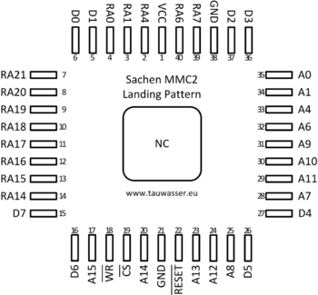
Sachen's MMC2 can be used to address up to 32 Mbit of ROM. It contains provisions for SRAM access.
Contents
Pinouts
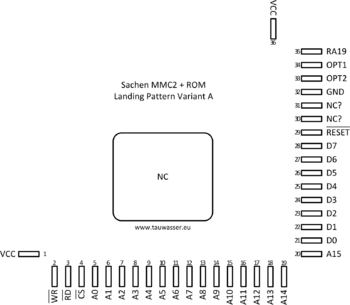
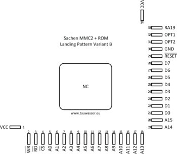
| Pin No. MMC2 | Pin No. MMC2+ROM A (MMC2+ROM B) | Name | Type | Comment |
|---|---|---|---|---|
| 1 | 1, 36 (34) | VCC | PWR | 5V supply |
| 21, 38 | 32 (30) | GND | PWR | Ground supply |
| — | (30–31) | NC? | N/A | Unused pin. |
| 6–5, 37–36, 27–26, 16–15 | 21–28 | D0–D7 | I | Data Bus |
| — | 3 | RD | I | Low-Active Read Enable |
| 18 | 2 | WR | I | Low-Active Write Enable |
| 19 | 4 | CS | I | Low-Active Chip Select |
| 22 | 29 | RESET | I | Low-Active Asynchronous Reset |
| 35–32, 28, 25, 31–29, 24–23, 20, 17 | 5–20 | A0–A15 | I | Address Bus |
| 4–2, 40 | — | RA0, RA1, RA4, RA6 | O | Scrambled lower ROM Address Lines |
| 39 | — | RA7 | O | Lower ROM Address Lines |
| 14–7 | 35 (33) | RA14–RA21 resp. RA19 | O | Upper ROM Address Lines |
| — | 34–33 (32–31) | OPT1–OPT2 | I (PD) | Option Input Pins |
| — | — | NC | N/A | Not connected. |
Theory of Operation
Sachen's MMC2 mappers are used for multi-game N-in-1 cartridges. Individual game ROMs can be remapped so their address space logically starts at ROM bank 0x00 although the individual ROMs might be stored starting at another bank. To avoid copyright infringement the game headers are scrambled and the mapper unscrambles them when the header region is read. The mapper also includes a mechanism to switch out the Nintendo logo with a custom logo while still passing the Game Boy Bootstrap logo check. All of these features are also used by various games as a copy-protection mechanism, e.g. ROM mapping, unscrambling and the logo in VRAM are checked to determine if the game is run from an original Sachen cartridge.
Sachen added a detection method for Game Boy Color to successfully perform the logo switch, since the Game Boy Color changed the way the logo is checked.
Modes of Operation
Sachen MMC2 has three modes of operation locked DMG, locked CGB and unlocked. It defaults to locked DMG after reset.
This is used to display the Sachen logo instead of the Nintendo logo for the DMG and CGB bootstrap ROMs. Because the DMG bootstrap copies the logo first and checks after displaying it, while the CGB bootstrap checks first and only afterwards uses the actual logo, Sachen devised a mechanism to detect a CGB using the fact that the CGB bootstrap writes to WRAM, while the DMG bootstrap doesn't.
While in locked DMG and unlocked modes, RA7 will follow A7. While in locked CGB mode, the mapper will keep RA7 set.
The unlock sequence is 0x30 transitions of A15 from low to high to go from locked DMG mode to locked CGB mode. Starting on the last transition, RA7 will remain set. Going from locked CGB mode to unlocked mode requires another 0x30 transitions of A15 from low to high. Starting on the last transition, RA7 will follow A7 again. The MMC2 mapper will skip directly from locked DMG mode to locked CGB on a rising edge of CS. The A15 transition counter is reset when changing from locked DMG to locked CGB mode.
Other functionality seems to be unaffected by the lock register: switching banks and remapping work while locked.
The only way to lock the mapper after unlocking is to reset it.
Header Scramble
Sachen chose to scramble the header of their games. When A8 is high, while A15..A9 are low, the mapper will perform the following map:
RA0 <= A6
RA1 <= A4
RA4 <= A1
RA6 <= A0
When A8 is low or A15..A9 are not low, RAn lines will track their respective An line.
Multi Memory Remap
Base ROM Bank and ROM Bank Mask Register are used for remapping 0x0000-0x7FFF to be based on a new base ROM bank.
The mapping function is:
(rb & ~mask) | (mask & rb_base)
Memory Map
- 0x0000-0x3FFF: Mapped ROM bank #0
- 0x4000-0x7FFF: Mapped Switchable ROM bank
- 0x8000-0xFFFF: Unmapped
Mapped here means adjusted for absolute Base ROM bank.
The RAn pins depend solely on A14, thus they will alias the 0x0000-0x7FFF region to 0x8000-0xFFFF. ROM is still only enabled when A15 is low, so no output is produced.
Registers
Write-Accessible Registers:
- 0x0000-0x1FFF: Base ROM bank register
- 0x2000-0x3FFF: ROM bank register
- 0x4000-0x5FFF: ROM bank mask register
ROM Bank Register
The ROM bank register is zero-adjusted, i.e. if 0x00 is written, 0x01 will be stored. Zero-adjustment is done on all 8 input bits D7..D0. This means, that ROM Bank 0x00 can only be mapped to 0x4000-0x7FFF when the attached ROM is smaller than 32 Mbit and thus aliases 0x80 to 0x00.
D7 D6 D5 D4 D3 D2 D1 D0    0x01 @ reset
\_____________________/
      \___/      \-------- ROM Bank
        |
        \----------------- Map Enable
ROM Bank bits switch the bank mapped to 0x4000-0x7FFF. Map Enable bits are used to enable write access to the #Base ROM Bank Register and #ROM bank mask register. 0b11 means these registers can be written, other values will not grant write access.
The width of this register is based off the fact that there are eight high address lines on the SA8MBT6-2 w/o BAT PCB.
Base ROM Bank Register
This register stores the base ROM bank.
D7 D6 D5 D4 D3 D2 D1 D0    0x00 @ reset
\_____________________/
                 \-------- Base ROM Bank
This register is writable without limitation when Map Enable in the #ROM Bank Register is 0b11. Changes to this register take immediate effect.
ROM bank mask register
This register stores the ROM bank mask.
D7 D6 D5 D4 D3 D2 D1 D0    0x00 @ reset
\_____________________/
                 \-------- ROM Bank Mask
This register is writable without limitation when Map Enable in the #ROM Bank Register is 0b11. Changes to this register take immediate effect.
Behavior
Integrated ROM
The integrated ROM behaves as a regular ROM chip that's connected to the An resp. RAn address and Dn data lines.
ROM chip enable behavior is:
#ROM_CS = A15 or RA20 or OPT2
The highest address line (RA18) will behave as follows:
RA18 = MMC1_RA18 or OPT1


